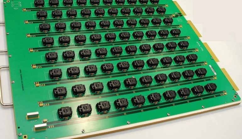
Burn-In Board
In the PCB industry the term ‘Burn-in Board’ is very common but if you’re just getting into the industry you might be scratching your head a little as to what one is!
We’ve been making burn-in boards for Semiconductor companies all around the world since 1994 -it’s like second nature to us. So, we thought we’d explain them for you in a little more detail….
Burn-In Process
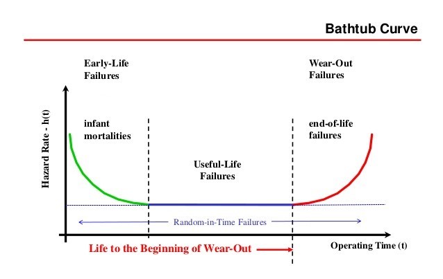
First of all, ‘burn-in’ is a process where semiconductor components are stress tested in order to detect any early failures due defects in design, materials, process or manufacturing .
The tests that are run will try to trigger possible failures that could happen in the real world and improvements can be made if necessary. Very often the semiconductor components are pushed beyond what they will have to go through in reality to allow for additional headroom. This ensures the manufacturer can be confident they have a robust end product.
The ‘Bathtub Curve’